集成电路设计
集成电路设计代写 Sketch the transistor-level schematic and the corresponding stick diagram of the following functions: Sketch another…
-
Sketch the transistor-level schematic and the corresponding stick diagram of the following functions: 集成电路设计代写
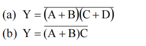
- Sketch another corresponding stick diagram of the functions:
 Compare with the stick diagram in 1(b) and explain which is better.
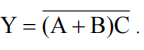
- Figure 1 shows the layout of an inverter. If the n-well must be at least 6 from the n-diffusion of the nMOS, determine the minimum inverter height (in terms of ) using the MOSIS SUBM design rule. 集成电路设计代写
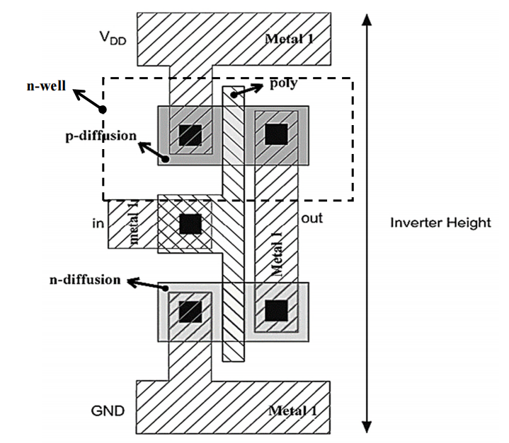
Figure 1
- The layout shown in Figure 2 is an n-channel enhancement type MOSFET device with the source and drain diffusion regions surrounded by channel-stop diffusion. Assume a CMOS process, draw well labelled cross-sectional diagrams along the A-A’ and B-B’ lines.
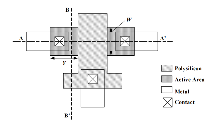
Figure 2
- (i) Draw the circuit diagram for the layout shown in Figure 3 and deduce the function, f , of the circuit.
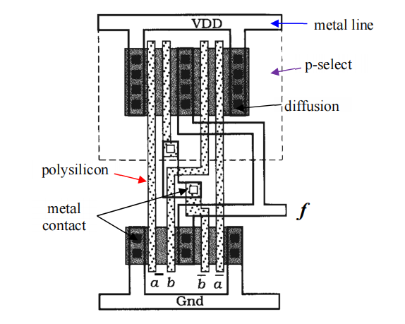
Figure 3
(ii) The circuit implementation for the 2-input function of part (b)(i) is not an intelligent design. Improved on the circuit design by re-evaluating the circuit function or by providing an alternative circuit configuration.